In fact, four-layer PCB reverse engineering is to repeatedly copy two double-sided PCB boards. Six layers is to duplicate three double-sided PCB boards… Multiple layers are scary. Because we can’t see the trace inside it. A precise multilayer PCB board, how do we see its inner wiring?
The main approach is to layer.
There are many ways to layer now, there are potion corrosion, cutting tool stripping and so on. But it’s easy to overdo the layers and lose data. Experience tells us that sanding with sandpaper is the most accurate.
When we reverse engineer the top and bottom layers of the PCB. It is generally sanded with sandpaper. Grind off the top layer to reveal the inner layer. The sandpaper is the ordinary sandpaper we buy in the store. Generally put the PCB board, and then hold the sandpaper. Rub the PCB evenly (if the board is small, you can also lay the sandpaper flat and rub the PCB against the sandpaper with one finger). The point is to smooth it so that it can grind evenly.
Screen printing and green oil are generally wiped off. The copper wire and the copper skin should be wiped a few times. Generally speaking, the bluetooth board can be wiped in a few minutes, and the memory bar is about ten minutes. Of course, the more strength, the less time it takes; It takes a little more time.
Grinding plate is the most common scheme used for layering at present. It’s also the most economical. We can find an abandoned PCB to try, in fact, there is no technical difficulty in grinding the board, but it is a little boring, it takes a little effort, and you don’t have to worry about grinding the board to your fingers.
In the process of PCB copy, after the system layout is completed, the PCB diagram should be reviewed to see whether the layout of the system is reasonable and whether it can achieve the optimal effect.
PCB reverse engineering can usually be investigated from the following aspects:
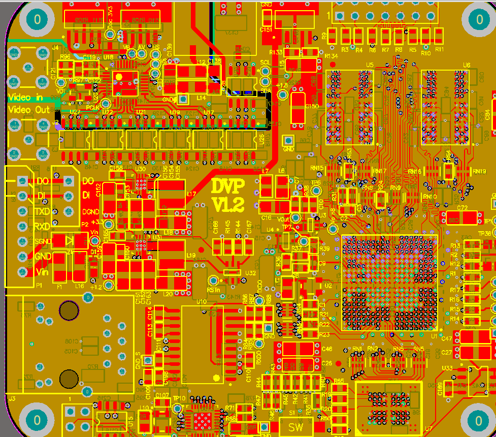
The picture below shows reverse engineering of an 8-layer PCB board. And it comes with a BGA chip. This is a complicated project. Our Shenzhen OROD Technology spent four days to complete PCB reverse engineering!
1. Whether the system layout ensures reasonable or optimal wiring. Whether it can ensure the reliable wiring, whether it can ensure the reliability of the circuit work. The layout requires an overall understanding and planning of the signal direction and the power and ground network.
2. Whether the size of the printed board is consistent with the size of the processing drawing. Whether it can meet the requirements of PCB manufacturing process, whether there is a behavior mark. This point needs special attention, many PCB board circuit layout and wiring are designed very beautiful, reasonable. However, the precise positioning of the positioning connector is neglected. As a result, the designed circuit cannot be docked with other circuits.
3. Whether there are conflicts between electronic components in two-dimensional and three-dimensional space. Pay attention to the actual size of the electronic components. Especially the height. In welding layout-free electronic components, the height generally cannot exceed 3mm.
4. Whether the layout of electronic components is orderly and neatly arranged. Whether all layouts are complete. When placing components, not only the direction of the signal and the type of signal should be considered. Need to pay attention to or protect the place, but also to consider the overall density of electronic components layout, to achieve uniform density.
5. Can the electronic components that need to be replaced frequently be easily replaced? Whether the plug-in board is convenient to insert the device. Convenient and reliable replacement and connection of frequently replaced electronic components should be ensured.
Anyway, multilayer PCB reverse engineering is a very troublesome job. Engineers are required to have sufficient experience and relevant electronic skills. The circuit diagram made in this way will not be wrong!

Leave a comment